The microstructure of the coating and the influence of the production process on it are critical factors in the design of optical coatings. This technical paper explores how the coating process can be influenced by environmental factors and the growth modes employed in vapour deposition coating.
When designing high performance thin films, it can be a mistake to assume that they will possess the same properties as the bulk material. The properties of thin films in reality can depend significantly on the temperature of deposition, the crystalline phase of the deposited material and moisture in the film among countless other factors. Ignorance towards such factors can have catastrophic consequences on coating quality, leading to unwanted shifts in spectral behaviour, reduced LIDT, reduced bandwidths or even stress-induced crazing. The first step in understanding and accounting for these technicalities is to understand the fundamentals of film growth.
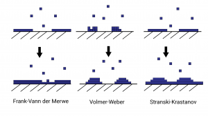
In physical vapour deposition thin films are produced via the condensation of a vapour incident upon a substrate. The atoms and molecules from the vapour stick to the substrate (as adatoms and admolecules), undergo nucleation and grow, eventually coalescing into a complete film after between around 1 to 20nm of growth. There are three principal growth modes depending on the surface energies involved.
Growth Modes
- Volmer-Weber (islands)
- Frank-Van der Werwe (layered)
- Stranski-Krastanov (layered + islands)
Volmer-Weber growth consists of initially small islands that grow and coalesce into a larger structure which occurs when interactions between the admolecules are stronger than that of the admolecules with the substrate. Frank-Van der Werwe growth occurs in the case where the admolecules are more strongly attracted to the substrate than eachother and form a lattice matching that of the crystal structure of the substrate. This results in the growth of successive 2d monolayers. Stranski-Krastanov is a hybrid of the other two growth modes in which one or two monolayers form, followed by 3d island growth. Volmer-Weber growth tends to be the most frequent process of nucleation when it comes to optical coatings.
As the islands grow, those islands with the lowest energy per atom have a tendency to subsume higher energy islands, reducing the total surface energy. This process repeats and the islands grow until the surface is covered, forming a polycrystalline network of grains separated by grain boundaries.

One of the important features of the coating deposition process to keep in mind is the fact that deposition takes place under highly metastable, non-equilibrium conditions, meaning that layers tend to grow dynamically as they try to transition to a lower energy state and may undergo recrystallisation processes or experience competitive grain growth as differing crystalline orientations compete with each other.
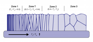
After the mean percolation thickness (the thickness at which islands coalesce into a more continuous film) the film continues to grow, sometimes for several hundred more nanometres should the coating design demand it. As the film grows it will typically develop a polycrystalline structure with a specific crystallographic orientation (sometimes referred to as texture), though the ultimate structure is heavily dependent on the ratio of the film material melting point Tm and the substrate temperature Ts. As Ts varies, various processes influence the structure.
Processes Influencing Thin Film Structure
- Shadowing – A low temperature effect where peaks on a rough substrate surface tend to accumulate more admolecules than valleys resulting in a rougher coating.
- Surface and Bulk Diffusion – Admolecules obtain increased mobility across the surface as the temperature increases and are able to fill grain boundaries. At even higher temperatures admolecules can diffuse into the bulk of the material.
- Recrystallisation – A complete change in crystal orientation. Dominant at high temperatures.
The Structure Zones of Thin Film Growth
With these effects in mind we can identify three structure zones as well as additional transitional states with increasing Ts.

At low temperatures (Ts/Tm< 0.3) incoming admolecules stay put due to neglible diffusivity and grow into a highly porous/columnar, underdense structure characterised by geometric shadowing of the substrate.
At higher temperatures surface diffusion is more dominant and voids/grain boundaries are filled. Between zones 1 and 2 we can identify a transitional zone T which, while denser than zone 1 suffers from weak texture as different crystalline orientations compete with one another. Zone 2 structure growth occurs at temperatures (Ts/Tm> 0.3) at which a single crystalline orientation emerges and grains are even more tightly packed.
At an even higher temperature (Ts/Tm> 0.5) zone 3 growth occurs and both types of diffusion are highly prominent. Due to the increased bulk diffusion the structure consists of rough, equiaxed grains with a scale comparable to the actual film thickness itself.
For typical optical coatings a tightly packed film with properties similar to the bulk (presumably amorphous) material are desirable. Achieving this however is a far from easy process.
References and Further Reading
Structure and Properties of thick condensates of Ni, Ti, W, Aluminium oxides and ZrO2 in vacuum, B.A. Movchan, A.V. Demchishin, Fiz. Metal. Metalloved. 28: 653-60, Russia (1969)
Thin Film Optical Filters Third Edition, H. A. Macleod, Institute of Physics publishing, J W Arrowsmith LtD. Bristol, 2001, ISBN 0 7503 06887 2
Microstructural evolution during film growth. I. Petrov et. Al. Journal of Vacuum Science & Technology A – J VAC SCI TECHNOL A. 21. 10.1116/1.1601610. (2003)

