Optical coatings are integral to the performance and durability of modern laser systems, yet they present unique challenges due to the stresses that can arise during their fabrication and use. Understanding these stresses – whether mechanical, thermal, or chemical – is crucial for ensuring the reliability and longevity of coated optics.
This technical paper delves into the complexities of stress in optical coatings, offering analysis of its origins, effects, and mitigation strategies. By exploring both the fundamental principles and practical considerations, the paper aims to provide valuable insights for anyone working with high-performance optics and to understanding their coatings.
The presence of stress within thin films presents a very real challenge in optical coatings as it can adversely affect coating adhesion, cause bending in the substrate (introducing unwanted aberrations) or possibly even lead to a catastrophic failure of the coating. In severe cases, stresses can be of such magnitude that they are of the order of GPa. Knowing is half the battle however and a keen awareness of the mechanisms that cause stress and stress-induced failures is the first step in combating it.
The total mechanical stress within a thin film σ is composed of three components:
σ = σext+ σtherm + σint
The term σext represents stress from external sources, and σtherm is the thermal stress caused by the difference between the thermal expansion coefficients of the film and substrate and is given by:
σtherm = Yf(af – as)(Tp – Tm)
Where Yf is the young’s modulus of the film, af and as are the thermal expansion coefficients of the film and substrate respectively, Tp and Tm the temperatures taken during measurement and during the coating process respectively.
The most complex and important component of the stress is the intrinsic stress arising from the film microstructure and growth. It exists in two principal forms, tensile stress due to the film contracting parallel to the substrate and compressive stresses due to the film expanding parallel to the substrate. Tensile stress has a tendency to induce cracks in the film that in some cases may even transfer to the substrate whereas compressive stress causes buckling and delamination of the film. Due to the complexity of intrinsic stress and its dependency on the deposition process there exist many models which provide useful but incomplete pictures of stress description.
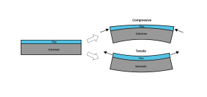
Figure 1: The two stress states and the resultant bending of the substrate.
Intrinsic stress arises from a variety of sources such as lattice defects, variations in interatomic, contamination, phase transformations and interactions at grain boundaries or voids to name a few. Packing density and the resultant microstructure play a big role. A film with pronounced columnar growth or polycrystalline structure and low packing density will experience strong tensile stresses due to forces between grain boundaries/columns. Conversely films with a closely packed micro-structure tend to be under compressive stress. Additionally, even amorphous or polycrystalline films with a higher packing density experience tensile stress due to the attractive forces present within voids, cavities and grain boundaries. In some cases, moisture filling the voids can reduce tensile stress or even convert it into compressive stress!
Analysing the evolution of stress during film growth also gives insight into the nature and origins of thin film stress. As an example we can consider the Volmer Weber (V-W) growth mode. Consider an initially bare substrate with a flux of evaporated material incident upon it. Initially the material will form lone islands, a process known as “nucleation”. Over time these islands grow and eventually intersect and coalesce signifying the formation of grain boundaries. This process continues until the film becomes relatively flat and uniform, at which point it begins to grow in thickness. The behaviour of stress throughout these three processes follows a “CTC” (compressive-tensile-compressive) pattern typical for high mobility films. The islands cause compressive stress initially until they begin to coalesce and the stress is tensile until atoms are driven into grain boundaries, returning the film to a compressive stress state.
The stress is also dependent on the material utilised in conjunction with the process, for example pure metal films are generally under tensile stress though the exact value depends on the method of production. Metal oxides are capable of showing either stress state though they tend to be compressive under energetic processes. Thick SiO2 films produced via electron-beam evaporation show compressive stresses of around 160MPa, though sub-100nm thick films can show extremely high stresses of up to 1.1GPa.
The primary method of countering tensile stress is of course the utilisation of energetic or sputtering methods (Electron Beam PVD, Magnetron Sputtering, Ion Assisted Deposition) as this results in a higher packing density and a less columnar micro-structure though in some cases this pushes the film stress from tensile to compressive! Encouraging the growth of larger grains also results in a reduced tensile stress. Generally speaking, thicker films tend to be under lower intrinsic stress.
Figure 2: Photograph of a coating which has buckled under stress
References and further reading
Thin Film Optical Filters Third Edition, H. A. Macleod, Institute of Physics publishing, J W Arrowsmith LtD. Bristol, 2001, ISBN 0 7503 06887 2
Optical Interference Coatings, N. Kaiser, H. K. Pulker, Springer-Verlag Berlin Heidelberg 2003, ISBN 3-540-00364-9
Moisture adsorption in optical coatings, H, A. Macleod, NASA, Ames Research Center, Second Workshop on Improvements to Photometry USA, NASA, Ames research Centre (1988), p. p 303-320
Stresses and Failure Modes In Thin Films And Multilayers, J. W. Hutchinson, Division Of Engineering And Applied Sciences, Havard University, Cambridge, MA 02138, USA (1996)
Review Article: Stress in thin films and coatings: Current status, challenges, and prospects, J. Vac. Sci. Technol. A 36, 020801 (2018); https://doi.org/10.1116/1.5011790